Table of Contents
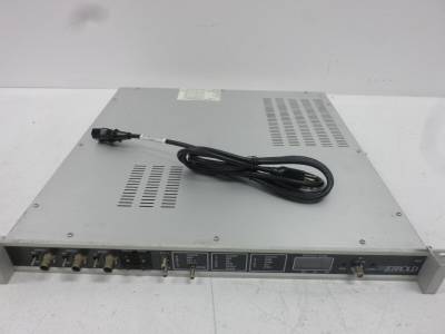
Jerrold MVP baseband scrambler
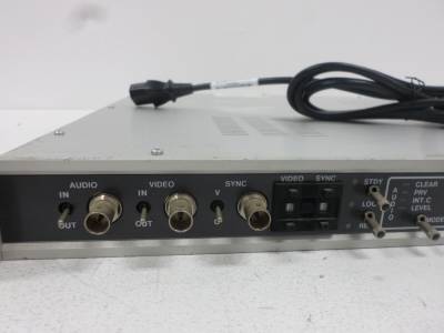
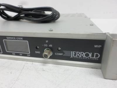
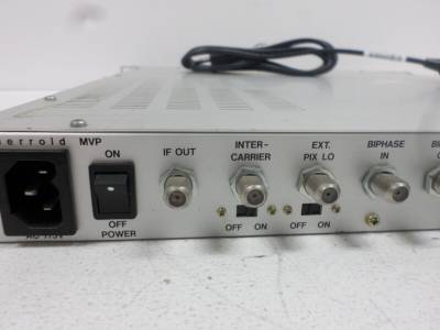
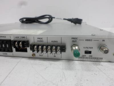
The MVP, or “Modulating Video Processor” is a combined modulator and video scrambler.
The MVP accepts baseband composite NTSC video and audio as inputs, applies sync-suppresion and video-inversion scrambling, and outputs modulated video at a 45.75 MHz IF. The IF-out may then be connected to a suitable upconverter and launch amplifier.
There was a variant, the “MVP-PAL”, which accepted PAL video instead of NTSC. I'd like to obtain one of these units, or find out more about the differences between it and the standard (NTSC) MVP. If you happen to know anything about the MVP-PAL, please contact me.
MVP (original, "Mk.1")
Option DIP switches
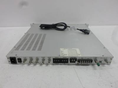
The Option DIP switches are located on the rear panel, below the Aux/GND screw terminals.
| Option | 1 | 2 | 3 | 4 | 5 | 6 | 7 | 8 |
|---|---|---|---|---|---|---|---|---|
| RF | 0 | 0 | 0 | 0 | x | x | x | 0 |
| Baseband | 1 | 0 | 0 | 0 | x | x | x | 0 |
| Mixed | 0 | 1 | 0 | 0 | x | x | x | 0 |
| SSE | 1 | 1 | 0 | 0 | x | x | x | 0 |
| Alternate | 0 | 0 | 1 | 0 | x | x | x | 0 |
| Special | 1 | 0 | 1 | 0 | x | x | x | 0 |
| Timing Camouflage | 0 | x | x | x | x | 1 | x | 0 |
| Data Camouflage | 0 | x | x | x | x | x | 1 | 0 |
| Alignment | 0 | 0 | 0 | 0 | 1 | 0 | 0 | 0 |
- Up: 0
- Down: 1
- Don't care: X
Scrambling modes
- RF: none, 6dB or 10dB sync suppression with no inversion or audio privacy. Data is sent as AM modulation of the FM audio carrier. Compatible with RF terminals. Emulates the DSE Digital Scrambler Encoder.
- Baseband: none, 6dB or 10dB sync suppression with optional video inversion. Data is sent as 3.58MHz bursts on VBI lines. Compatible with Baseband terminals. Emulates the VPE Video Processor Encoder.
- Mixed: None, 6dB or 10dB sync suppression. Data is sent as both AM modulation of the FM audio carrier, and VBI data. Video inversion and audio privacy are disabled. Compatible with both RF and Baseband terminals.
- SSE: Emulates the Starpack Scrambler/Encoder. Allows 6dB sync suppression, no video inversion, and no audio privacy. Compatible with Starpack and RF terminals.
- Alternate: Used with Hamlin encoders to place AM timing data on the sound carrier. No video inversion or audio privacy. Use only with Hamlin compatible RF converters.
- Timing Camouflage: RF mode only. Inserts false timing pulses to confuse pirate descramblers.
- Data Camouflage: RF mode only. Inserts false data to confuse pirate descramblers.
Sync switch settings
| Switch position | Sync scrambling mode |
|---|---|
| 0 | Clear |
| 1 | 6 dB |
| 2 | 10 dB |
| 3 | Scene change – 16 fields |
| 4 | Scene change – 3 seconds |
| 5 | Dynamic – 15 seconds |
| 6 | Dynamic – 30 seconds |
| 7 | Dynamic – 60 seconds |
| 8 | Dynamic – 16 fields. Linear change, for test purposes only. |
| 9 | Clear |
| A | |
| B | |
| C | |
| D | |
| E | Clear. In remote mode: firmware revision displayed on Service Code Indicator. |
| F | Clear. In remote mode: Remote Address displayed on Service Code Indicator. |
Video switch settings
| Switch position | Video scrambling mode |
|---|---|
| 0 | Clear |
| 1 | Constant inversion |
| 2 | Scene Change switching – 16 fields |
| 3 | Scene Change switching – 3 seconds |
| 4 | Dynamic – 15 seconds |
| 5 | Dynamic – 30 seconds |
| 6 | Dynamic – 60 seconds |
| 7 | Dynamic – 16 fields. Linear change for test purposes only. |
| 8 | Clear |
| 9 | |
| A | |
| B | |
| C | |
| D | |
| E | |
| F |
Internal settings
- SW304 (rear of PCB, in audio section): Audio input impedance. “600” for 600-ohm balanced audio, “50k” for 50k unbalanced audio.
- SW303 (front part of audio section): Unknown. Set to “On”.
- SW302 (middle part of audio section): Unknown. Set to “On”.
- Switching to “Off” causes attenuation of audio above ~10kHz.
- Treble boost? Pre-emphasis on/off?
- SW202 (rear part of video section): Unknown. Set to “Off”.
- Switching to “On” attenuates audio.
- Audio attenuator?
Hardware
- Main processor: Mitsubishi MELPS-740 variant with internal Jerrold Biphase receiver/transmitter (GIC 135-062-003, 968-100, 946104)
- ROM: 27C256
- Realtime clock: Oki MSM62X42B
Memory map
| Start | End | Function |
|---|---|---|
0000 | 00FF | (CPU internal?) Zero page RAM |
0100 | 01FF | (CPU internal?) Stack RAM |
4400 | 440F | Oki MSM26X42B RTC nCS0: U17 (74HCT32) pin 8 CS1: tied to Battery Backed VCC nWR: white PAL pin 16 nRD: white PAL pin 15 RTC read and write are fully-decoded (only active when nCS0 is active). nCS0 is active when either nWR or nRD are active. |
4800 | U1 (74HC245). Rear panel OPTION dip switches, low 8 bits. DIR=0, OE=yellow PAL pin 19. |
|
4801 | U3 (74HC245). Rear panel REMOTE ADDRESS BCD thumb-wheel MSBs. DIR=0, OE=yellow PAL pin 18 |
|
4802 | U2 (74HC245). Rear panel REMOTE ADDRESS BCD thumb-wheel LSB, and SERVICE NUMBER BCD thumb-wheel MSB. Low nibble: Remote Address LSB. High nibble: Service Number MSB DIR=0, OE=yellow PAL pin 17 |
|
4803 | U4 (74HC245). Rear panel SERVICE NUMBER BCD thumb-wheel LSBs. DIR=0, OE=yellow PAL pin 16. |
|
4C00 | U5 (74HC245). Front panel, VIDEO and SYNC hex thumb-wheel switches. Low nibble: SYNC High nibble: VIDEO DIR=1, OE=yellow PAL pin 15 |
|
4C01 | Front panel 7-segment LED display, left digit | |
4C02 | Front panel 7-segment LED display, middle digit | |
4C03 | Front panel 7-segment LED display, right digit | |
5000 | 5007 | Interface FPGA I/O, functions unknown |
8000 | FFFF | 27C256 EPROM Chip select: not-A15 from U43 (74HC04) pin 8 Output enable: PHI2 clock from CPU pin 31 |
U6 (74HC245) – address not known. DIR = RAM /WE, OE = white PAL pin 18. “B” bus connects to the CPU/RAM/ROM data bus. “A” bus connects to the other 74HC245s and the front panel board.
Thumb-wheel switches
The switches have pull-up resistors, and have their common pin connected to ground. To get the selected value in binary form, invert the value read from the port.
Seven-segment LED display
The firmware contains a table which maps a binary code to segment data values:
| Input | Character | Segment Code |
|---|---|---|
| 0-9 | Digits 0-9 | 48, F9, 8C, A8, 39, 2A, 0A, F8, 08, 38 respectively. |
| 10 | Blank | FF |
| 11 | F | 1E |
| 12 | P | 1C |
| 13 | U | 49 |
| 14 | S | 2A |
| 15 | b | 0B |
| 16 | y | 29 |
The segment data bits map to a byte as follows:
 A
F B
 G
E C
 D   *

*=decimal point

Segments:  FGED*CBA
Bits:      76543210
MVP-II
The operation manual for the MVP-II is (at the time of writing) available from http://systemindustrialgroup.com/Enter/support/MVP_op.pdf.
Biphase remote control port
The MVP communicates with a headend controller using the Biphase In and Out ports on the back panel. The data format is Manchester-encoded data, in the same format and at the same data rate as the Jerrold FM data channel commands used to send commands to cable receivers. For more on the FM data channel format, see GI/Jerrold FSK data format.
The input circuit is an LM311 comparator with a 75-ohm terminated input and a threshold of around 1V.
The output driver is a SN75158 which feeds the Biphase output port via a 75-ohm series resistor.
As the voltage levels in use are (broadly) 0V/5V, it is possible to drive the input and output with an Arduino or similar 5V-powered processor.
MVP logical address
The MVP's logical address may be set between 260097 and 260999 (3F801 hex to 3FB87 hex, or 774001 octal to 775607 octal) using the BCD thumbwheel switches on the back panel.
The following code can convert the decimal logical address to and from the four-byte logical address sent over the biphase network:
void mvp_addr_to_la(const uint32_t addr, uint8_t *la)
{
	// NOTE: The address entered on the MVP's panel and on the ACC is one higher than the address in the packet.
	uint32_t real_addr = addr - 1;

	// encapsulate the LA
	la[0] = 0xE0;	// geocode 0-7
	la[1] = 0xBF;	// octal 77 => headend equipment
	la[2] = 0x40 | ((real_addr >> 6) & 0x3F);	// LA high 6 bits
	la[3] = 0x00 |  (real_addr & 0x3F);			// LA low  6 bits
}


uint32_t mvp_la_to_addr(const uint8_t *la)
{
	uint32_t real_addr = 0;

	// NOTE: The address entered on the MVP's panel and on the ACC is one higher than the address in the packet.

	real_addr  = ((uint32_t)la[3] & 0x3F);
	real_addr |= ((uint32_t)la[2] & 0x3F) << 6;
	real_addr |= ((uint32_t)la[1] & 0x3F) << 12;
	real_addr |= ((uint32_t)la[0] & 7) << 18;

	return real_addr + 1;
}
Return packet format
Return packets (on the MVP's Biphase Out port) have the following format:
- IRG bytes (at least one), all 0xFF
- Packet length in bytes
- Four-byte logical address (sender address)
- Data payload
- Two's complement checksum (sum of all bytes in the packet and the checksum should be zero)
- XOR checksum (XOR of all bytes in the packet, the two's complement checksum, and the XOR checksum should be zero)
Where return data from a command is described below, only the payload contents will be described.
Commands
The following commands are understood by the MVP:
Headline
FD 41: Read
FD 60: Set clock
| Outgoing command bytes: | 0xFD 0x60 (year) (month) (day) (hour) (minute) |
|---|---|
| Response payload bytes: | None |
| Field | Contents |
|---|---|
year | Current year, modulo 16. Valid range is 0 to 15. |
month | Current month. Valid range is 0 to 11. |
day | Current day. Valid range is 0 to 30. |
hour | Current hour. Valid range is 0 to 23. |
minute | Current minute. Valid range is 0 to 59. |
Sets the MVP scrambler's realtime clock.
FE: Reset
| Outgoing command bytes: | 0xFE (LA3..LA0) |
|---|---|
| Response payload bytes: | None |
This command causes the addressed MVP scrambler to reboot.
